Revision
Electronic devices are different from Electric devices. The electric devices are the fundamental passive elements: resistor, inductor and capacitor. Electronic devices include the semiconductor devices.
The current known electronic devices are:
- Diode
- Normal
- Light
- Zener
- Transistors
- BJT
- FETs
- MOSFETs
- JFETs
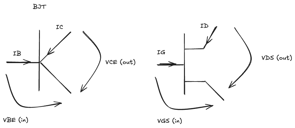
Transistor notations:
Examples
Diode circuit
In this example we'll solve a circuit with diodes. This will be an approximate solution as we will not be using the characteristic equation.
Circuit and notations
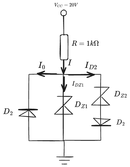
Proprieties of the circuit elements:
- $V_cc$ = 20 v
- $D_1 \equiv D_2$ ($I_0$= 10 nA)
- $D_{Z1}$ :
- $V_{Z1}$ = 18 v
- $I_0$ = 100 nA
- $D_{Z2}$ :
- $V_{Z1}$ = 5 v
- $I_0$ = 100 nA We must find the bias point for each diode.
Suppositions
Assume $D_1$ is off. Assume $D_2$ is on. Assume $D_{Z1}$ is off. (From KL1) Assume $D_{Z2}$ is on.
Circuit analysis
Since $D_1$ and $D_{Z1}$ are off, their saturation current, $I_0$ and $I_{DZ1}$ will flow through the circuit. Moreover because the saturation currents are very small we can approximate as follows: $$ I_{0}, I_{DZ1} \ll I \Rightarrow I \approx I_{D2} = I_{DZ2} $$ Now we can solve the circuit using KL2:
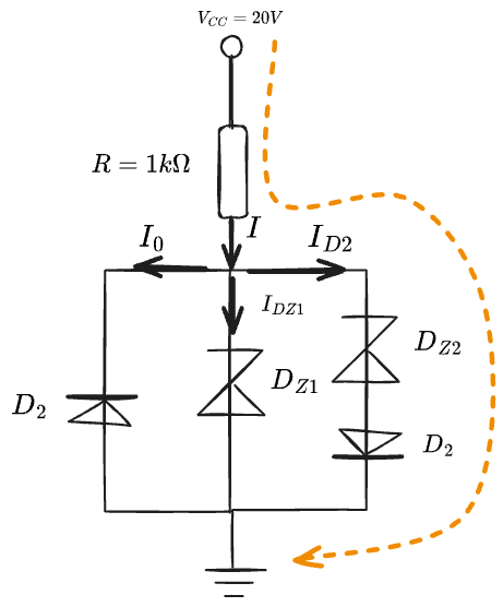
$$V_{cc} -0 = IR + V_{DZ2} + V_{D2} \Leftrightarrow I = \frac{V_{cc} - V_{DZ2} - V_{D2}}{R} = \frac{20-5-0.6}{1K}$$
And the final value of $I_{D2}$ is 14.4 mA. Using this we can easily solve the rest of the circuit and bias the diodes.
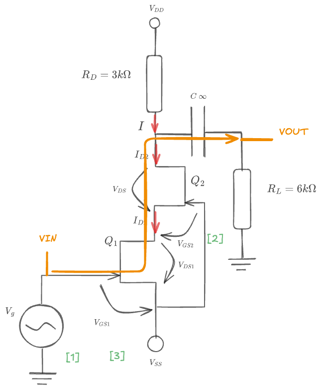
FET Circuit
Circuit and notations
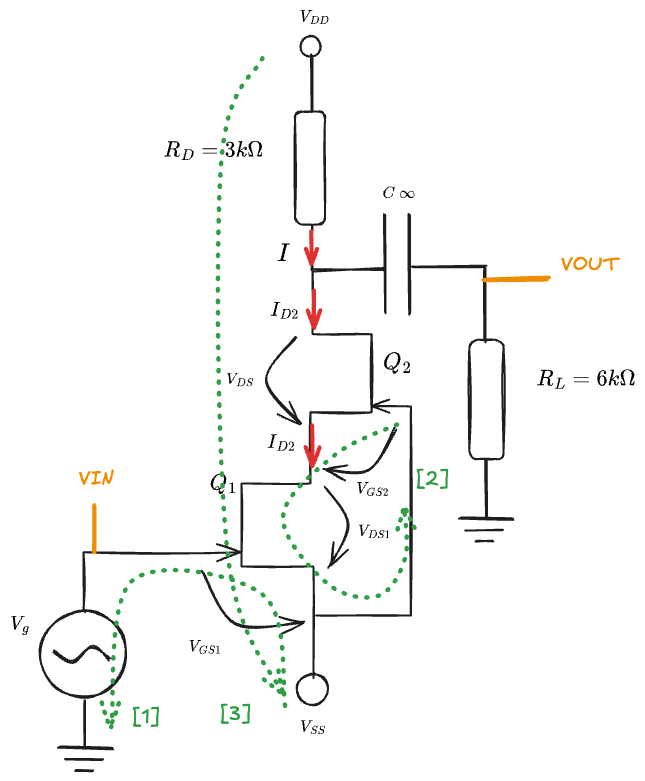
Circuit analysis
DC-OP
Our goal in DC-OP is to find $V_{DS1}$ and $V_{DS2}$,
We can safely assume that: $$ (1) \quad I \approxeq I_{D1} \approxeq I_{D2} $$ Since the current is flowing through the same branch; Now let's apply KL2 on the loop $[1]$: $$ V_{ss}+V_{GS1} = 0 \Rightarrow V_{GS1} = -V_{SS} = -2\text V $$ And this voltage must be negative for FETs so its all good. Now remember that the FET transistor characteristic equation: $$ I_D = I_{DSS} (1-\frac{V_{GS}}{V_T})^2 $$ Because of $(1)$, we can compute and write: $$ I_{D_{1,2}} = 10\text{mA} (1-\frac{(-2)\text{V}}{(-3)\text V})^2 = 2\text{mA} $$ Moreover, writing explicitly the equations gives us the actual value for $V_{GS2}$: $$ \begin{cases}I_{D1} = I_{DSS} (1-\frac{V_{GS1}}{V_T})^2 \ I_{D2} = I_{DSS} (1-\frac{V_{GS2}}{V_T})^2 \ (1) \end{cases} \Rightarrow V_{GS1} = V_{GS2} = -2 \text V $$ Now for the loop $[2]$, to find $V_{GS2}$ we apply KL2. Note that for this loop there are only two voltages in this loop. $$ (2) \quad V_{GS2}+V_{DS1}=0 \Rightarrow V_{DS1} = -V_{GS2} = 2\text V $$ And finally, let's find $V_{DS2}$ from loop $[3]$: $$ V_{DD}-V_{SS} = I R_{D}+V_{DS1} + V_{DS2} \Rightarrow V_{DS2} = 4\text V $$ We have successfully found that: $$\begin{cases}V_{DS1}=4V \ V_{DS2}=2V\end{cases}$$ This concludes the DC-OP.
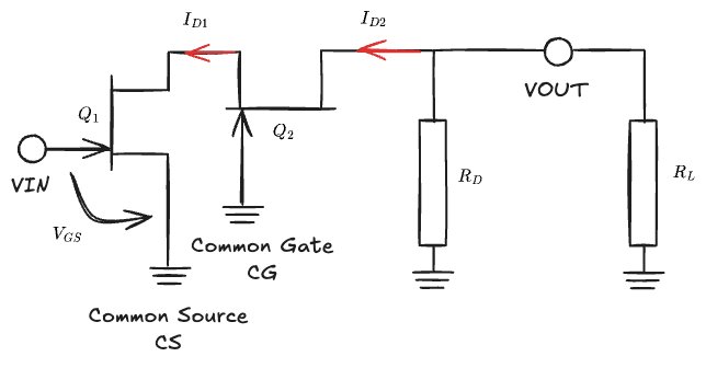
AC analysis
For the AC analysis we are going to follow the path from the Input Point to the Output Point.
Note that in AC Small Signal (what do we have right now) the $C\infty$ capacitor behaves like a short circuit.
From this path we can draw the AC scheme:
Let's compute the voltage gain $A_v$. By definition $A_v$ is the ratio between the output voltage $V_\text{OUT}$ and input voltage $V_\text{IN}$: $$ A_v = \frac{V_\text{OUT}}{V_\text{IN}} $$ Now we just play with the ratio to find ratios that we can compute: $$ A_v = \frac{V_\text{OUT}}{I_{D_2}}\frac{I_{D2}}{I_{D1}}\frac{I_{D1}}{V_{GS}}\frac{V_{GS}}{V_\text{IN}} $$ Let's have a look into the rations we've chosen
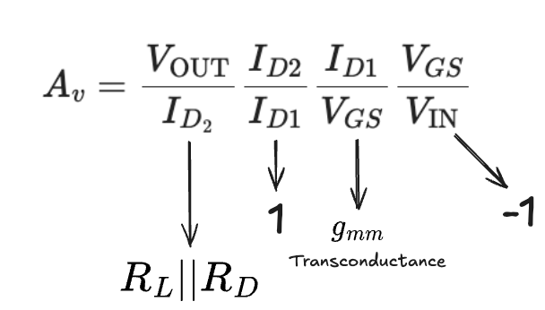
$g_\text{mm}$ is called transconductance and is computed using the following formula (for FET's): $$ g_{mm} = \frac{2\sqrt{I_\text{DSS}I_\text{D}}}{|V_T|} = 4kS $$ Back to the voltage gain $A_v$: $$ A_v = (-1)g_\text{mm}(R_L || R_D)$$ Now let's compute the resistances:
$R_\text{IN}=R_G = \infty$
$R_\text{OUT}=R_G || R_D || R_L = R_L || R_D$ And that's it.